What Lies Beneath the Surface
UT researchers have succeeded in manipulating the electronic behavior of a one-atom-layer-thick sheet material, without compromising its chemical composition or structural integrity. Using a technology known as “modulation doping,” they exposed a hidden “quantum matter phase” whose stability and properties are controlled by charges originating from the supporting silicon template. These findings, reported today in Nature Communications, provide a compelling proof of principle in that complex quantum phenomena with potentially important applications in electronics and information technology can now be realized and tuned on the technologically important silicon-based materials platform.
Quantum mechanics describes (sub)atomic-scale systems and explains, for instance, how atomic nuclei decay or how lasers work. The microelectronics industry has been revolutionized by scientists’ ability to control the properties of electronic materials restricted to three dimensions. Researchers are going even smaller by studying two-dimensional materials and ultimately getting down to a single layer of atoms, known as the two-dimensional quantum limit. Arguably, the most famous example is graphene, a single layer of carbon atoms that’s ultra-light, strong, and flexible. Yet, when the system gets smaller, the physics changes.
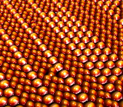
An STM image at right shows two different coexisting surface phases in a single layer of tin atoms on a silicon substrate. The larger “bowls” represent the high-temperature phase, whereas the smaller ones represent the low-temperature phase. The relative abundance depends on temperature and doping level of hole-doped samples. The work is described in a March 7 Nature Communications paper.
Scientists have successfully tailored the properties of materials by tinkering with their structure. Say you have a silicon wafer. Every silicon atom has four valence electrons where each electron partners with a valence electron of a neighboring atom, thus forming a chemical bond. Now add a minute amount of arsenic. An arsenic atom has five valence electrons, meaning every arsenic atom adds one extra, unpaired electron to the mix. This is called electron doping. Conversely, you could add boron instead of arsenic. With only three valence electrons, every boron atom leaves one space where there’s no partner for a silicon electron. This is called hole doping. This sort of musical chairs arrangement works well for three-dimensional materials, allowing access to phases like magnetism and superconductivity. It has had mixed success when the dimensions shrink to two because simply adding dopants to these more confined systems often destroys whatever functionality scientists were hoping to gain.
In the Nature Communications paper, Postdoctoral Research Associate Fangfei Ming and colleagues found a novel approach to resolve this issue. They started with four silicon wafers, doping one with arsenic and the remaining three with boron. Then they covered each with a single layer of tin atoms—the system of interest. They experimented with a wide range of temperatures and doping concentrations, using a scanning tunneling microscope (STM) to see what happened. They discovered that when boron atoms were placed in the silicon layer far enough away to avoid bonding with the tin atoms but close enough to steal some of their charge, the result was a rare displacive-insulator to insulator transition in the tin layer. Further, the tin layer was in no way compromised in terms of its chemical structure. Physics Professor Hanno Weitering, one of the paper’s authors, explained what that transition means.
“Simply put, displacive means that at low temperature, one atom has moved up while another one (typically its neighbor) has moved down, all in an orderly fashion,” he said. “At room temperature, all atoms typically have equivalent height, or as in the present case, exhibit a distinctly different buckling pattern.
“At room temperature, the tin layer has a polar symmetry,” he continued, just like a ferroelectric material. Imagine that a pair of atoms looks like a dumbbell, where one side has a positive charge and the other side has a negative charge, with an arrow pointing from the negative end to the positive end. In a ferroelectric material, all the arrows point in the same direction. This direction can be flipped by applying an electrostatic field.
“In our case, that is not possible because the lattice symmetry of the substrate (the silicon base layer) forbids this switch,” he said. “The substrate spoils the fun.”
The arrows are in one direction at room temperature, but at low temperature, one line of arrows points one way while the neighboring lines point in the opposite direction.
“If you would ignore the substrate, our system looks like an antiferroelectric at low temperature and a ferroelectric at high temperature,” Weitering said. The “antiferroelectric” phase would have remained hidden if not for a bit of serendipity related to the tools of this particular experiment.
“We are often interested in phases that have some exotic properties, for instance superconductivity,” he explained. “However, we have to work with what mother nature provides us. A hidden phase cannot be accessed by, for example, varying the temperature or applying a magnetic field, so they easily escape detection. You have to use a trick to find them.”
In this case, Ming, Weitering, et al found that “kicking the system” with the tip of the scanning tunneling microscope was the trick that worked. An STM uses a probe to move across the surface of a sample to create a contour map. Electrons tunnel between the sample and the probe, generating an electric signal. In the Nature Communications research, the current from the tip prompted the displacive phase transition in the hole-doped sample. Curiously, this “tip assist” doesn’t work for electron-doped systems, a study for further investigation.
The results show it’s possible to alter the physical processes on the tin surface while keeping its composition pristine, thus avoiding the common pitfalls of doping two-dimensional materials.
The paper, “Hidden phase in a two-dimensional Sn layer stabilized by modulation hole doping,” is available online. Authors include Fangfei Ming and Hanno Weitering, as well as Daniel Mulugeta (physics postdoc), Weisong Tu (physics graduate student, now UT alumnus), Tyler S. Smith (physics graduate student), UT Physics Research Scientist Paolo Vilmercati, Geunseop Lee of Inha University in Korea, Ying-Tzu Huang and Renee D. Diehl of Penn State University, and UT Physics Joint Faculty Assistant Professor Paul C. Snijders. Weitering, Vilmercati, and Snijders are also affiliated with the UT-Oak Ridge National Laboratory Joint Institute for Advanced Materials.